
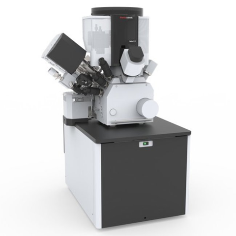
"Wind River": Focus Ion Beam/Scanning Electron Microscope
CASI houses the Thermo Scientific Helios 5 UX DualBeam Focus Ion Beam/Scanning Electron Microscope (FIB-SEM) to accelerate nanotechnology research and development at the University of Wyoming. This advanced instrument offers nanoscale sample preparation and three-dimensional characterization capabilities. Its fusion of industry-leading focused ion beam and electron beam performance, along with exclusive software and automation, ensures ease of use and precision for SEM imaging, FIB etching/deposition, e-beam lithography, and chemical analysis in 2D and 3D. The system is capable of various sample preparations and advanced analysis, including porous analysis for rock samples for oil and gas reservoirs, high-resolution S/TEM sample preparation for semiconductors, atom probe tomography (APT) sample preparation, and 3D elemental analysis for advanced materials. This instrument was funded by the Wyoming Innovation Partnership.
Instrument Highlights
- High-Quality Sample Preparation:
Achieve the highest-quality, site-specific, ultra-thin samples for transmission electron microscopy (TEM) and atom probe tomography (APT) using the groundbreaking Phoenix Ion Column with unmatched low-voltage performance.
- Automated TEM Sample Preparation:
Benefit from fully automated, unattended, multi-site in situ and ex-situ TEM sample preparation using optional AutoTEM 5 Software, ensuring precision and productivity.
- Advanced Imaging:
Experience the fastest access to nanoscale information with the Elstar Electron Column featuring SmartAlign and FLASH technologies, allowing users of all experience levels to obtain the finest details.
- Unmatched Materials Contrast:
Utilize next-generation UC+ monochromator technology for sub-nanometer performance at low energies, revealing sharp, refined, and charge-free contrast from integrated detectors.
- Multi-Modal 3D Characterization:
Obtain the highest-quality subsurface and 3D information with optional Auto Slice & View 4 (AS&V4) Software, offering precise targeting of regions of interest for accurate characterization. This includes advanced Energy-Dispersive Spectroscopy (EDS) capabilities for chemical analysis using the Pathfinder Alpine EDS System, enabling 3D chemical analysis.
- Piezo-Driven Stage:
Navigate with high precision using the five-axis motorized stage with a Piezo-driven XYR axis, ensuring accurate sample positioning and manipulation.
- E-beam lithography:
The system is integrated with an E-beam lithography package and NPGS lithography system.
Specifications
| Electron Optics |
Elstar extreme high-resolution field emission SEM column |
| Schottky thermal field emitter | |
| SmartAlign technology for user-alignments-free operation | |
| Electron beam current range: 0.8 pA to 100 nA | |
| Accelerating voltage range: 350 V – 30 kV | |
| Landing energy range: 20 eV – 30 keV | |
| Beam deceleration with stage bias from 0 V to -4 k | |
| Ion Optics |
Phoenix Ion Column with superior high-current and low-voltage performance |
| Ion beam current range: 1 pA – 65 nA | |
| Accelerating voltage range: 500 V – 30 kV | |
| 23-position aperture strip | |
| SEM resolution |
0.6 nm at 15-2kV |
| 0.7 nm at 1kV (with beam deceleration | |
| 1nm at 500V (with Beam deceleration and ICD) | |
| FIB resolution |
4.0 nm at 30 kV using preferred statistical method |
| 2.5 nm at 30 kV using selective edge method | |
| 500 nm at 500V using preferred statistical method | |
| Detectors |
ETD-traditional Everhart-Thornley Detector for detecting secondary and backscattered electrons |
| TLD-Through the Lens Detector for detecting secondary electrons, backscattered electrons | |
| ICD – In-Column Detector for detecting backscattered electrons | |
| MD - Mirror Detector for detecting backscattered electrons | |
| ICE – Ion Conversion and Electron – for detecting secondary electrons and secondary ion | |
| Retractable, low-voltage, high-contrast, directional, solid-state backscatter electron detector (DBS | |
| Gas Chemistry |
Platinum deposition |
| Tungsten deposition | |
| Lithography | E-Beam with NPGS system |
| Location | Science Initiative Building 1315 |
| Fee | Located in Rates |
Contact Info & Location
Instrument Manager: Qian Yang, qyang3@uwyo.edu
Instrument Location: Science Initiative Building 1315
The University of Wyoming has earned its Research Level 1 (R1) status from the Carnegie Classification of Institutions of Higher Education, placing Wyoming's only four-year university with the top research universities in the United States.